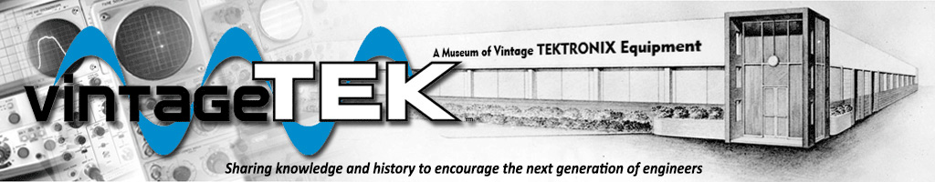
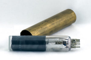
More photos and information are on the 200 Series Oscilloscopes on-line exhibit page. This working handmade "miniscope" prototype was important in the 200 series initial development. Dave Allen restored it to working condition after almost 50 years of being ignored.
It’s hard to remember as it has been 50 years. In 1968, I came to work in the Advanced Circuits Design group of Hiro Moriyasu as a summer student. I had already built a kit scope and had built an oscilloscope of my own design before coming to Tektronix. I remember being impressed with the Sony/Tek 321 and the idea of a scope in a probe with this 1" CRT was something I was very interested in.
Howard Vollum and Bill Walker would come around now and then and I'm sure the idea of a new line of miniature oscilloscopes was discussed in staff meetings that included Howard, Bill, Hiro and others. When returning to Tek after graduation, I must have been assigned to work on the new "miniscope" project.
As a new engineer in a big company, it was like being in “heaven” with a stock room the size of my living room with every component an engineer could desire. I had the best oscilloscope that money could buy and many more fantastic instruments. I started collecting things to build a 1” scope in a probe. I was ready to engineer something great.
I knew only a little about all the support that Tek could provide, like CRT engineering, Industrial Design, Mechanical Engineering, Prototype Fab, ECB layout, Ceramics, many more support groups and willing component suppliers. I'm sure that Hiro was the one to contact all those groups to get things going (obviously with the influence of the "Advanced Circuit Design Group” and a comment like "Howard wants it"). All the conceptual prototypes were made by the Industrial Design group and each week we had another small model to look at. Some were made of cardboard and Styrofoam and others were shaped, painted, with see through tops and had actual turning knobs. I don’t recall exactly how the final format of the 200 series came about, but it had a good size control panel , a place to store the probe and a tilt stand for easy viewing - a more practical version of the futuristic previous models.
At that time, Tek had just brought up a new "LSI" analog IC fab facility and was looking for new designs. I started designing ICs for a small scope. The IC lab would provide two or three actual IC transistors in an eight pin package. I used many transistor packages to build and test the proposed design just using the IC transistors, a few resistors and NO capacitors. After showing that the prototype circuit worked, the circuit diagram was turned over to the IC mask layout group and after two or three weeks all the layers of the diffusion masks were cut on 4 foot by 6 foot rubylith sheets to be photo reduced for the diffusion masks of the new IC. After another week or so, I was given a handful of actual ICs and they worked just like the handmade prototype. I developed a total sweep circuit IC, a vertical amplifier IC and an output IC, each in separate ICs
The only 16 pin IC package available at the time was a dual inline packag that was about 1" long and too big for a real "miniscope". We came up with a small 1/4" round IC with 16 radial leads that sat in a hole in the ECB and was hand soldered in. Tek didn't like ICs soldered in so the IC packaging area developed a 16 pin square package that could be plugged in and we went with that. At the time, surface mount components were just being introduced, but Tek didn't have the means to place them and Tek didn't think they would be all that reliable, so we used standard miniature components (for components that had be outside the ICs) and took advantage of the Tek ceramic resistor networks for the precision resistors.
As rotary switches were way too big for such a small miniscope, we developed a small rotary switch with contacts that would ride on the gold runs of the ECB. I think the Cam-switch was being developed at that time. We made the switch logic etched right on the ECB. We had switch wafers on both sides of the ECB and for a while, we had "half way through" feed-throughs so we could get layer two connected to the switch on layer one and layer three connected to layer four without messing up the other sides. ECB Fab didn't like the "half way feed-throughs" so we changed the switch layout to make them happy.
ECB layout was right down the hall and with a schematic, a drawing of the outline , the experience of a good layout person and some over the shoulder suggestions, in about a week, a four layer ECB was all taped and ready for photographic reduction. At that time there was a quick ECB fab in the basement of building 50 and if a set of film work was turned in that afternoon you had a completed ECB the next morning. How good could it be?
Two things I remember about the Model Shop in the basement of building 50 - aside from all the fantastic models they made for us. When we finally got a complete CRT to test, it needed a magnetic shield. Generally a shield of Mu-metal would be formed and spot welded together then annealed. Well, the model shop decided to see if they could deep draw a one-piece CRT shield from a single sheet of Mu-metal. They made the dies to do so and I remember watching them pressing the inner die onto the sheet of Mu-metal and drawing out a complete CRT shield in about three passes. It really worked. I don’t know why they didn’t use that process, probably because Tek didn’t have the proper equipment to build it in production, but the 200 series CRT shields were finally made just like the others, formed and spot welded together.
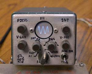
When we finally got all the parts for the first (pre-A phase) 211, we needed a plastic case to put them in. The mechanical design of the dies for the injection molded 211 enclosure was in progress, but it would be quite a while before the first parts could be molded. The Model Shop made two side panels by milling them out of thick plastic blocks. The top and bottom parts of the case were vacuum formed over quick aluminum molds and then trimmed to best represent the actual parts. It looked real crude, but for the first time we had an actual 211 “miniscope” to hold in our hand, run some initial tests and show off to all those who had contributed to its birth.
One of the first design goals was to have the 200 series of oscilloscopes be double insulated - to be “floatable”. We advertised it as “floatable” and several “tongue in cheek” comments came back that someone threw it in water but “IT PROMPTLY SANK!”. The double insulated feature of the “miniscope” is why it has the plastic case. Every part of the electronics inside that connected to the AC power lines have at least two layers of insulation between the internal circuits and anything a user can contact. The charging circuit, the batteries and the primary of the internal power supply all float on the AC power line. Since the ground of the input probe could be attached to the AC power lines, all of the circuitry inside the unit had to have the same insulation to the outside of the unit where a user might touch. We had to have extra insulated slide switch covers, plastic knobs without set screws and any access hole had to be small enough. Product insulation was not that hard for the 211 as it only had one ground lead for the probe. But for a dual trace 212 and 214 we had to have a yellow ground leads for the two probes with special instructions that these two leads are internally connected together and should be used with caution when floating the instrument.
I can remember going over to Plastics to watch them inject the first parts of the 211 enclosure. The white side panel worked just fine and we got several new parts. They had problems injecting the top and bottom of the case as the die would stick and not separate like it should have. They had a hard time getting the finished part out of the mold. As I recall, the problem was that the mold was not symmetrical left to right. The whole side where the side panel would fit was not there in the finished part. The mounting of the die in the injection frame had to take up the side pressure. I don’t know how they fixed it, but we finally got the top and bottom parts out of the mold.
One thing Tek always did with a new product was to test it out thoroughly to the EIS (Engineering Instrument Specification) that was initially drawn up and signed off by engineering, production, management ETC. I can just remember putting that little 211 in that horrid environmental chamber and cycling it between 0°C to 80°C at 98% RH – and it still worked!
As production built these 200 series “miniscopes” I kept track of how many they had built. When the 1000th 211 was just about to be built, I asked if I could get the 1000th unit to give to Howard Vollum. As Electro-chem could do almost everything, I took several of the 211 enclosures over and asked them to gold plate them. Well, the process for applying gold on plastic required a little more heat than the plastic could endure. Several of the cases were badly warped so I picked the best ones, applied a little heat and pressure and made one set look just fine. The next hurdle loomed. As we all know, gold is NOT an insulator. The inside of the enclosure was now connected to the beautiful gold plating all over the outside. A gold 211 might be lethal if you plugged it in while holding it. With a standard Dremel tool, I removed a path of gold on the inside of the case about ¼ inch wide all around the edge so the outside was only cosmetic and not connected to the inner part. It looked wonderful!. I always wondered what Howard did with it.
The 211 came first, the 212 was pretty much an upgrade to one of the ECBs and a new side panel. The 214 came next and included some special switches and two new circuit boards. It also needed a new storage CRT that CRT engineering provided. The 214 was a bit more effort. The 221 came next and as it was ten times faster, it took a lot of more engineering. None of the 211 ICs were fast enough so the 221 was all done with discreet parts. The discrete parts were crammed in and it took a bit more power.
By the time we got to working on the 213, I was mostly managing the group and I only did the battery charger design. We chose to use two D size batteries as there was about twice as much power in two D batteries as there was in same volume of AA size batteries. Driving a whole scope off of 2V was not easy. As the 213 had many different functions, there was a great designer assigned to each part. The 211 had two ECBs and to get all the functions of the 213 crammed into the same package, we needed six ECBs. All of the parts were on the inside of the four main ECBs (not one spare space was left unused) with only the ECBs showing when you took the 213 out of its case. In order to work on the 213 in production we had to develop 3 small ECBs and a long cable that would connect the four main ECBs together, lay them out flat, with the parts visible to be worked on. I’m sure production really hated this problem.
After the 213 was finished, we launched into developing a 20Mhz dual channel “miniscope” with a new eight by ten division screen CRT using the newly developed mesh scan expansion CRT. We even got a few new CRTs to try, but the spot size in the first prototypes was still a bit too big. Just as we were working up the specifications for the new higher bandwidth “miniscope” Tektronix took on a contract from Burroughs to build a digital test system (eventually called the 851). The year of the “mini” anything was the mid-1960s and early-1970s and I guess the new word was “digital” so the “miniscopes” ended and the “digital this or digital that” came into vogue.
There were so many great engineers and people who produced the Tektronix “miniscopes”. This photo of all those who we could find at the time is a great reminder of those great people. I wish I could name them all. I’m glad I was assigned to work on the first “miniscope” and I have enjoyed every year I worked at Mother Tektronix. Tek is not the same company now and at that time Tek could do anything and did almost everything.
David W. Allen
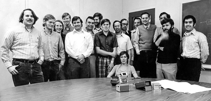
Jim Knowlton, 213 power supply design
Doug Morse, 221 input amplifier design
Bruce Campbell, 221 electrical design
Ron Henricksen
Unknown, possibly ECB layout
Possibly Eugene Wilson, mechanical design
Unknown
Wayne Thomas, 214 storage
Possibly Bill Cottingham, mechanical design
Gordon Meigs, 213 design
John Pace, 200 series early electrical design
David Allen, all 200 series electrical design and group manager
Wendell Damm, all 200 series electrical design
Howard Mehan, made the prototype models in industrial design
Iraj Nikzi, industrial design
Unknown (at desk), possibly ECB layout
If you recognize some of these people please let the museum know.