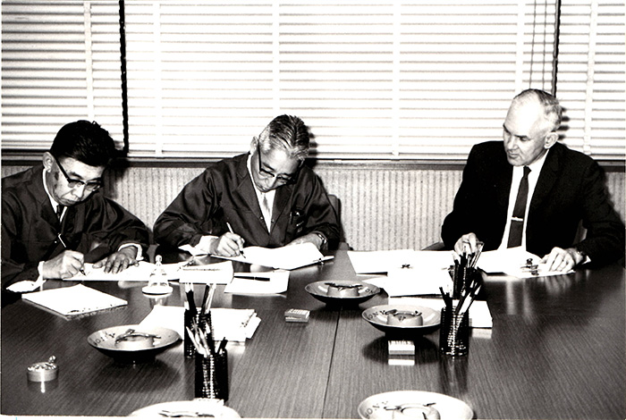
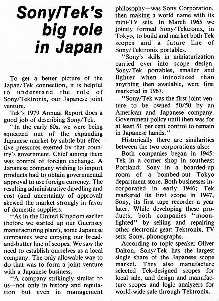
Tektronix management first thought about some type of venture in Japan in the late 1950s. They distributed products through Midoriya but the growth was slow. Japanese companies were copying Tektronix products and Tektronix wanted a direct presence in Japan. By 1963 they began conversations with Hitachi and Toshiba. While in Japan, Howard Vollum visited their customer Sony and was impressed with their chief engineer Dr. Masaru Ibuka. Later he met the founder Akio Morita and the two struck up a friendship. In 1964 Earl Wantland visited Sony to further discussions and in March of 1965 Tektronix and Sony struck a 50/50 partnership Sony/Tek.
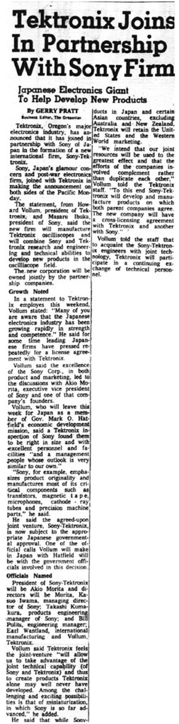
This November 9, 1964 Oregonian article describes the new relationship.
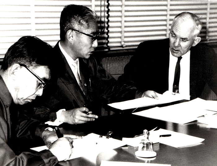
These two photos show Howard at the signing the official documents.
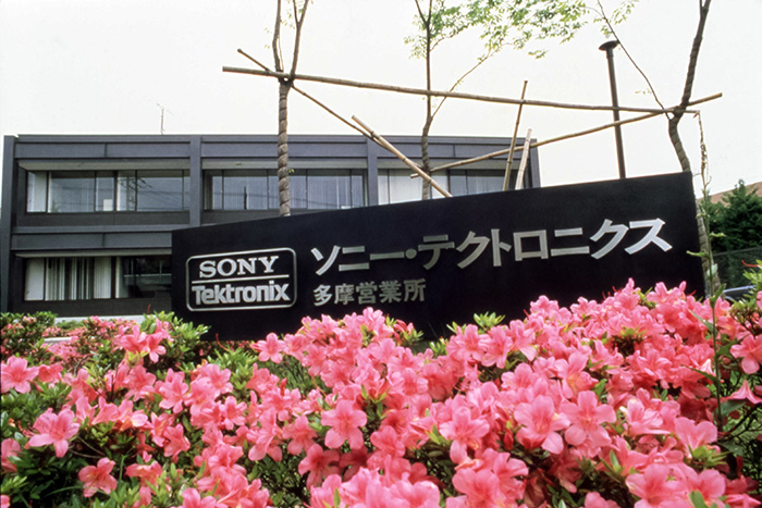
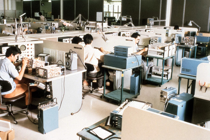
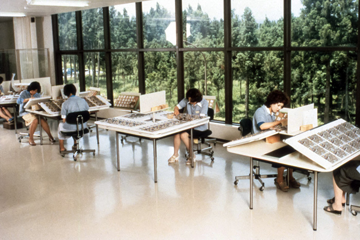
Sony/Tek began operations with headquarters, engineering, and manufacturing in a Sony building in Osaki. The original building is no longer there but the was close to 35.620529 139.731415. They began by building products using Tektronix components and assemblies and then developed their own products usually focusing on miniaturization and specialization for the Japanese market.
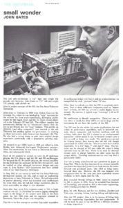
In May of 1965 John Gates was assigned responsibility for the first Sony/Tektronix development project, the design of the 323 mini-oscilloscope. This Summer/Fall 1968 TekTalk describes his contributions to Sony/Tek and the development of the 323 mini-oscilloscope. Click on the image to view the PDF.
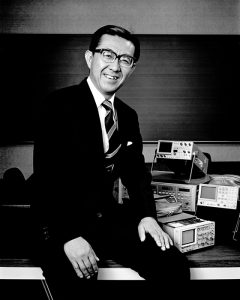
Sony/Tek President Takashi Kumakura. Products are 336, 318, 338, 380
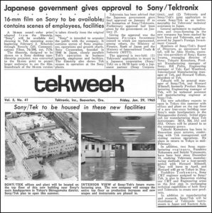
This January 29, 1965 issue of TekWeek features several articles on Sony/Tektronix. Click on the image to view the PDF.
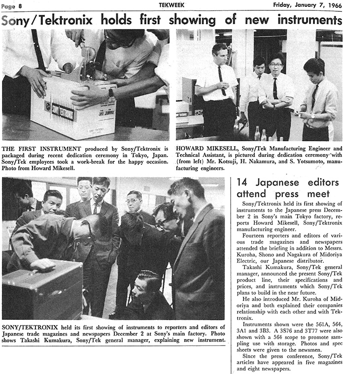
This January 6, 1966 issue of TekWeek features an article on the first products developed by Sony/Tektronix.
Sony/Tek built their own facility in 1969 which was a four story building that housed the entire operation. This October 3, 1969 TekWeek features an addition to the building.

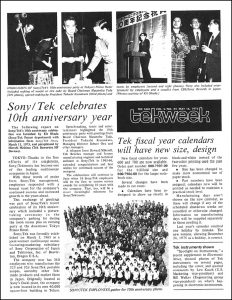
This May 16, 1975 issue of TekWeek describes the 10 year anniversary celebration of Sony/Tek. Click on the image to view the PDF.
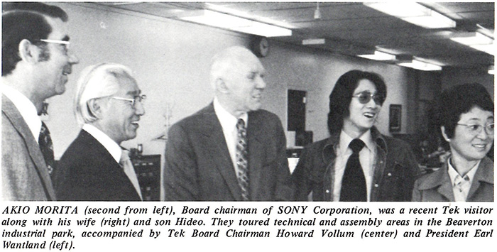
This June 11, 1976 Tekweek photo features a visit to Tektronix by Sony board chairman Akio Morita, his wife, and son.
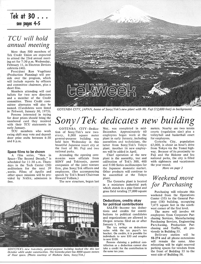
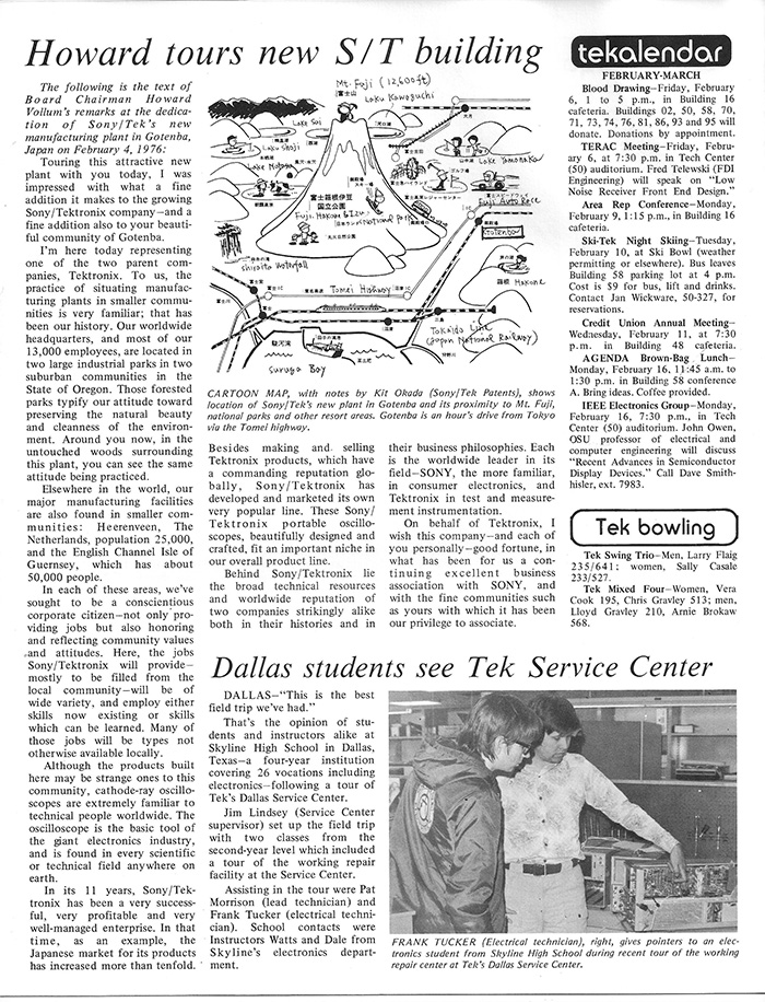
In 1976 they expanded with a new facility in Gotemba and moved manufacturing. These February 6, 1976 TekTalk articles describe the new facilities.
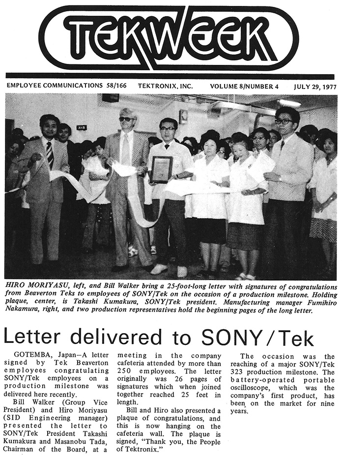
This July 29, 1977 issue of TekWeek is about a Sony/Tek milestone on the 323 battery operated oscilloscope. We have one on display in the museum.
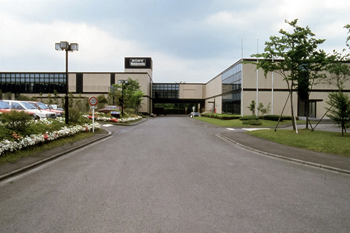
In 1980 Sony/Tek built a second eight story building next to the original building which had corridors connecting the two on the first three floors. Sony/Tek headquarters, the Tokyo field office, engineering, marketing, and the Information Display Group moved to the second building.
This August 28, 1981 TekWeek features some history of Sony/Tek.
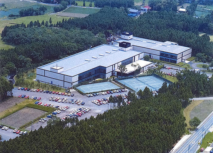
In 1983 Sony/Tek expanded the facility in Gotemba. In the time period from 1965 to 1990 sales expanded more than 10X. This photo shows the Gotemba facility with the original building on the right and the expansion on the left. The Gotemba building can be seen today on Google Maps by searching for "35.284408, 138.907316".
Sony/Tek President Takashi Kumakura visited Tektronix just prior to their 20th anniversary. This September 21, 1984 TekWeek features his visit. Click on the image to view the PDF.
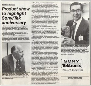
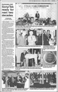
1985 marked the 20th anniversary of Sony/Tektronix. There were two issues of TekWeek on May 10th and June 21st highlighting the anniversary. Click on the images to view the PDF.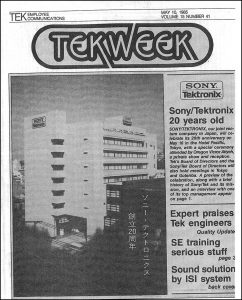
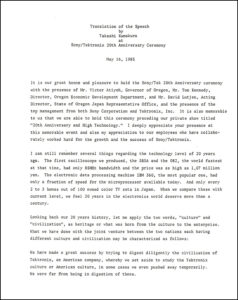
 This document is the translation of the speech given by Takashi Kumakura on May 16, 1985 at the 20th anniversary celebration. Click on the image to view the PDF.
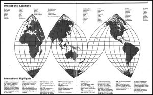
This excerpt from a summary of Sony/Tektronix was also produced in 1985 for the board meeting. Click on the image to view the PDF.
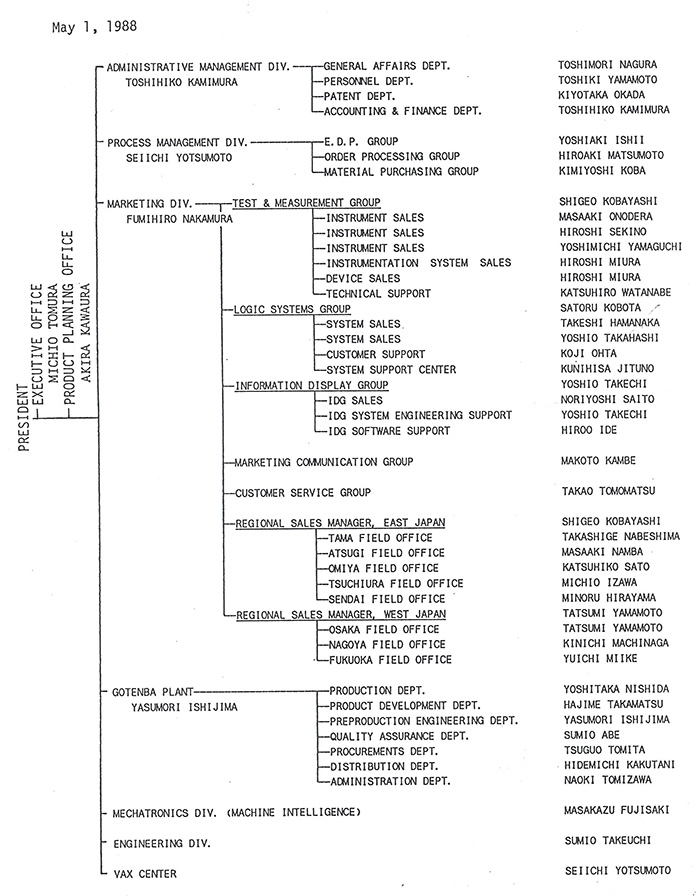
Here is an organizational chart for Sony/Tektronix from 1988
There is a 30th Anniversary of Sony/Tek booklet and a Memories of Gotemba booklet on our Articles page. We also have a Sony/Tek Products on our Exhibits page.
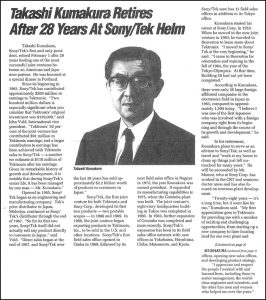
This February 13, 1993 TekWeek features an article on the retirement of Takahashi Kumakira retiring from Sony/Tek after 28 years. Click on the image to view the PDF.
Sony/Tek continued as a 50/50 joint venture until 2002 when Tektronix fully acquired the company as Tektronix Japan. Tektronix leveraged the sales and distribution arm of Sony/Tek but began to integrate other functions into the Beaverton organizations. Tektronix Japan moved to Shinagawa Intercity, the former Japan National Railway (JNR) yard at the east exit of Shinagawa Station. They occupied the 6th (sales) and 7th (engineering) floors of Shinagawa Intercity Building B. In 2005, manufacturing at Gotemba was shut down and the building sold.
Sony/Tek, and later Tek Japan, had engineering competencies in spectrum analyzers and waveform synthesis technologies. Eventually these skills and some resources were relocated to the Beaverton campus and engineering in Shinagawa was shut down in 2008.
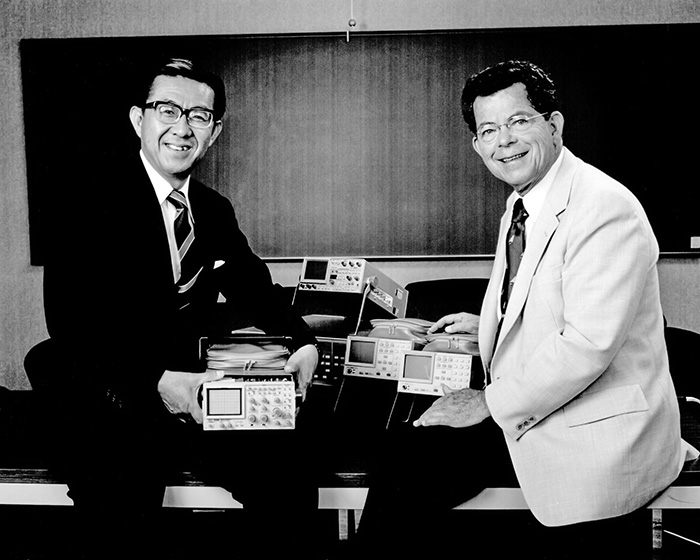 Sony-Tek president Takashi Kumakura with Lang Hedrick. Products are 336, 318, 338, 380